Introduction
Photonics systems operate at wavelengths measured in nanometers—visible light spans just 400 to 700 nm—making sub-micron machining precision essential at every stage of fabrication. A lateral misalignment of merely 1 µm between a fiber and edge coupler introduces 1 dB of excess loss, compromising signal integrity in telecommunications networks, targeting systems, and medical lasers. This scale challenge defines photonics component machining: the precision manufacturing of housings, mounts, and structural elements that hold and align optical elements in systems across aerospace, defense, medical devices, and telecommunications.
Many engineers hit a wall between standard machining capabilities and photonics requirements. Conventional precision machining targets tolerances of 10–20 micrometers — photonics applications routinely demand ±300 nm alignment for inverted tapers and surface finishes better than Ra 0.2 µm.
Temperature adds another layer of difficulty. Fluctuations during machining can erase dimensional accuracy at the micron level, and material choice becomes critical when aluminum's 23.6 ppm/°C thermal expansion coefficient can shift optical paths with even minor temperature changes.
This article breaks down what it actually takes to machine photonics components reliably — the tolerance specifications that keep beams on target, the materials that hold their dimensions under real-world conditions, and the alignment strategies that bridge the gap between machining precision and field performance.
TLDR: Key Takeaways
- Fiber-to-chip coupling requires alignment tolerances as tight as ±300 nm for inverted tapers to maintain insertion loss below 1 dB
- Material CTE mismatch drives alignment failure: titanium at 8.6 ppm/°C holds position nearly 3× better than aluminum at 23.6 ppm/°C
- Passive alignment tops out around 2 µm; active alignment with optical feedback pushes accuracy to 20–50 nm
- Optical mounting surfaces require Ra 0.2 µm finishes versus standard machining's Ra 3.2 µm to prevent micro-tilts
- Inspection requires temperature-controlled environments at 20°C ±0.1°C — measurement uncertainty must stay well inside the tolerance budget
Understanding Photonics Component Machining
What is Photonics Component Machining?
Photonics component machining produces the mechanical infrastructure—lens barrels, mirror mounts, fiber alignment housings, detector enclosures—that positions optical elements with extreme precision. This discipline is distinct from fabricating optical elements themselves through grinding and polishing. Instead, it focuses on creating the precision mechanical components that hold optics in exact spatial relationships.
These housings and mounts underpin every beamline, laser assembly, and optical instrument. When a lens is seated in a precision-machined barrel, the mechanical accuracy determines whether the system performs to specification or drifts out of focus under thermal load or vibration.
Why Precision Matters in Photonics
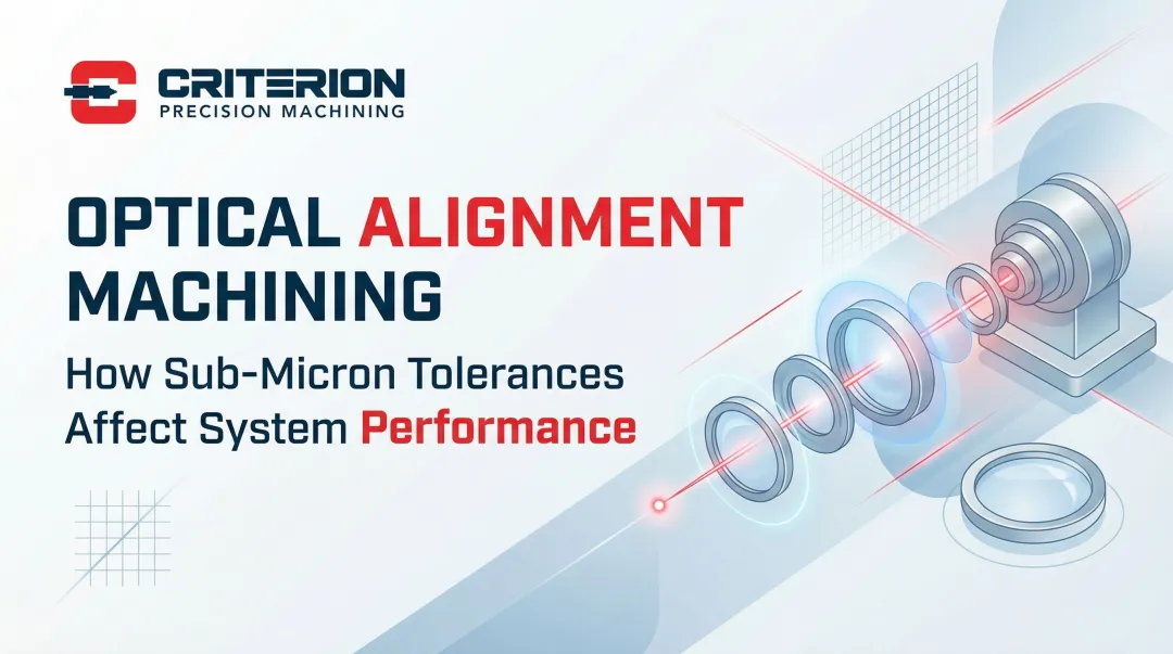
Mechanical tolerance directly governs optical performance. For Gaussian beams, a lateral misalignment of approximately 0.48 times the beam waist radius results in 1 dB loss. For a single-mode fiber with a 10 µm mode field diameter (waist ~5 µm), a shift of roughly 2.4 µm causes measurable performance degradation.
Angular errors compound over distance. A perpendicularity error of just 0.5° (8.7 mrad) creates an 8.7 mm lateral beam deviation over one meter—enough to miss a detector entirely or couple into the wrong waveguide channel. Fiber-to-chip coupling in silicon photonics illustrates these constraints: grating couplers require ±1 µm alignment to maintain insertion loss penalties below 1 dB, while inverted tapers demand ±300 nm precision.
Components That Require Precision Machining
Key component categories include:
- Lens tubes and barrels - Cylindrical housings with precision bores for lens seating and concentricity control
- Fiber optic connectors and housings - Alignment structures for single-mode and multi-mode fiber terminations
- Laser module housings - Enclosures that maintain optical alignment while managing thermal loads
- Mirror mounts and kinematic bases - Adjustable or fixed-position supports with angular stability
- Detector and sensor housings - Protective enclosures with precise aperture positioning
Criterion Precision Machining manufactures these components with tolerances down to ±0.0002" (±5 µm), routinely machining housings with tight concentricity requirements and complex bores to hold alignment within spec.
Industries Driving Photonics Component Demand
The same components appear across widely different end markets, each with its own mechanical and environmental demands:
- Telecommunications — Connector housings enable repeatable sub-micron coupling between fibers and transceivers across high-volume fiber optic networks
- Aerospace and defense — LIDAR systems, targeting optics, and rangefinders require thermally stable housings that hold alignment through temperature swings and shock loads
- Medical devices — Endoscopes, surgical lasers, and diagnostic imaging systems depend on biocompatible materials that maintain optical alignment in the body
- Quantum computing — Photonic quantum processors route and manipulate photons through integrated optics, where even nanometer-scale drift can compromise qubit fidelity
The Manufacturing Process Overview
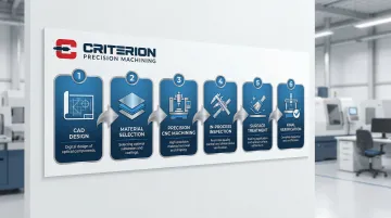
Photonics component manufacturing follows a disciplined sequence:
- CAD design - Optical engineers specify critical dimensions, geometric tolerances, and material requirements
- Material selection - Balancing CTE, machinability, weight, and optical compatibility
- Precision CNC machining - 3-axis, 4-axis, 5-axis milling and Swiss turning operations
- In-process inspection - Dimensional verification during machining to prevent scrap
- Surface treatment - Anodizing, coating, or finishing as required
- Final verification - CMM inspection with comprehensive dimensional reporting
Critical Tolerance Requirements in Photonics
The Sub-Micron Imperative
Photonics demands tolerances specified in microns or fractions thereof, compared to standard machining tolerances in thousandths of an inch (25.4 µm). Silicon photonics alignment requires accuracies between 20 and 50 nanometers for 0.02 dB coupling repeatability.
Application-specific tolerance ranges:
- Telecommunications (fiber coupling): ±5 µm for multimode, ±1 µm for single-mode
- Aerospace LIDAR: ±2 µm for beam steering accuracy
- Medical imaging: ±3 µm for endoscope lens trains
- Quantum photonics: Sub-100 nm for waveguide coupling
Geometric Tolerances: Beyond Linear Dimensions
Linear dimensions tell only part of the story. Geometric tolerances control the relationships between features:
- Perpendicularity - Optical axis alignment; 0.5° error creates 8.7 mm deviation over 1 meter
- Concentricity - Lens centering within barrels; typically specified to 5-10 µm TIR
- Surface flatness - Mounting surfaces require flatness within 2-5 µm across the surface
- Parallelism - Beam paths through multi-element assemblies demand parallel surfaces within 10 µm
When optical elements seat against these controlled surfaces, they hold their designed spatial relationships — no tilt, no decentration, no axial drift. Surface finish is where that precision either holds or falls apart.
Surface Finish Requirements
Surface texture affects seating stability and introduces micro-level misalignment. Standard machined surfaces typically achieve Ra 3.2 µm (125 µin), which is too rough for precision optical mounting.
Photonics finish requirements:
- General optical mounts: Ra 0.8 µm (32 µin) for dimensional control
- Precision interfaces: Ra 0.4 µm (16 µin) for critical seating surfaces
- Mirror-finish surfaces: Ra 0.025 µm (1 µin) for ultra-critical contact points
Roughness peaks create point contacts rather than continuous support, allowing micro-tilts that amplify into beam misalignment.
Thermal Considerations in Tolerance Management
Temperature variations during machining affect dimensional accuracy at the micron level. The international reference temperature for dimensional measurement is 20°C, with high-accuracy environments requiring stability of ±0.1°C and gradients controlled to 0.03°C/hour.
Consider what a 1°C swing actually means in practice:
- A 100 mm aluminum part expands 2.36 µm — nearly half the total tolerance budget for many photonics applications
- Steel expands roughly 1.17 µm over the same change; titanium about 0.86 µm
- Even brief thermal gradients during machining can permanently shift a feature out of spec
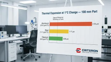
Temperature-controlled machining and inspection environments are essential infrastructure, not optional upgrades.
Criterion maintains temperature-controlled environments for achieving and measuring ultra-tight tolerances, recognizing that thermal consistency is fundamental to photonics precision.
Tolerance Stack-Up in Multi-Component Assemblies
Individual component tolerances compound in assemblies through tolerance stack-up. Three components with ±5 µm tolerances can result in ±15 µm total variation in worst-case analysis, exceeding many photonics system budgets.
Stack-up mitigation strategies:
- Use kinematic design to constrain exactly six degrees of freedom, eliminating over-constraint and stress-induced distortion
- Build in adjustment mechanisms so active alignment can compensate for mechanical stack-up after assembly
- Apply selective assembly — pairing a slightly oversized lens with a slightly oversized barrel, for example — to reduce effective variation without tightening individual tolerances
Statistical methods like Root Sum Squares (RSS) assume normal distributions and estimate probable variation, typically allowing looser individual tolerances while maintaining low failure probability.
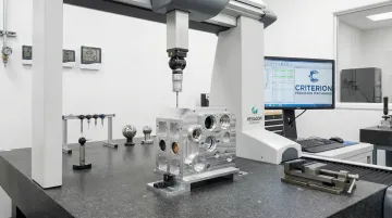
Inspection and Metrology Capabilities
Measurement accuracy must exceed part tolerance by at least 10:1 to ensure valid inspection. CMMs should be verified according to ISO 10360 standards to ensure they meet stated maximum permissible errors.
Essential metrology tools:
- Coordinate Measuring Machines (CMM) for 3D dimensional verification with sub-micron accuracy
- Optical comparators for non-contact profile measurement on delicate features
- Laser interferometry for nanometer-resolution measurement in ultra-precision applications
- Surface profilometers to verify Ra and texture to micrometer levels
Criterion uses a Global Advantage CMM with PC-DMIS software, capable of measuring complex geometries with repeatability sufficient for photonics tolerances. Their OASIS optical inspection system measures multiple dimensions simultaneously, while Keyence systems can measure up to 99 dimensions on 100 parts at once.
Materials Selection for Photonics Components
Key Material Properties for Photonics Applications
Material selection balances multiple competing requirements:
- CTE — controls whether the housing expands in sync with optical elements during temperature shifts
- Dimensional stability — resistance to creep and stress relaxation over time keeps alignment from drifting
- Machinability — not all materials can be held to sub-5 µm tolerances without specialized tooling
- Weight — drives material choice in aerospace, airborne LIDAR, and handheld systems
- Chemical compatibility — contact with optical adhesives, cleaning solvents, and coatings can degrade some materials
CTE mismatch between housing and optical element creates stress and misalignment during temperature excursions. A 20°C temperature change in a 50 mm aluminum housing (CTE 23.6 ppm/°C) produces 23.6 µm expansion—far exceeding typical alignment budgets.
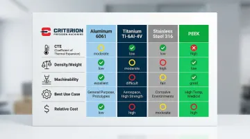
Aluminum Alloys: The Workhorse Material
Aluminum 6061-T6 and 7075-T6 are the default choice for most photonics housings. They machine cleanly, cost less than titanium or stainless, and at 2.70 g/cc keep system weight manageable. The modulus of 68.9 GPa is sufficient for most non-vibration-critical structures.
Where aluminum falls short is thermal stability. Its 23.6 ppm/°C CTE—already quantified in the expansion example above—means any application with wide temperature swings needs either tight thermal control or a different material.
Key trade-offs to weigh:
- Anodizes well for wear resistance and optical surface properties
- Lower stiffness than steel requires thicker wall sections to maintain rigidity
- Ultra-fine mirror finishes are achievable but demand diamond-turning or specialized finishing
Criterion machines 6061-T6 and 7075-T6 photonics housings to ±0.0002" using Swiss turning and CNC milling, with inspection via CMM to verify bore concentricity and datum relationships.
Titanium: For Demanding Aerospace and Defense Applications
When aluminum's CTE is too high for the thermal environment, Ti-6Al-4V is the next step. Its CTE of 8.6 ppm/°C sits much closer to optical glasses, and the strength-to-weight ratio rivals aluminum while adding superior corrosion resistance. That combination makes it the standard material for airborne LIDAR, space-based instruments, and defense targeting systems where neither weight nor dimensional drift is negotiable.
The trade-off is machinability. Titanium work-hardens during cutting, generates significant heat at the tool-chip interface, and accelerates tool wear—all of which drive up cycle times and cost. Maintaining ±0.0002" requires sharp tooling, controlled feed rates, and adequate coolant flow throughout the operation.
Stainless Steel: For High-Stability Applications
Where stiffness matters more than weight, stainless steel grades 303, 316, and 17-4PH take over. Grade 316 has a modulus of 193 GPa—nearly three times aluminum—and a CTE of 16.0 ppm/°C, which can be acceptable in thermally stable environments.
The penalty is density (8.00 g/cc) and cost. Stainless is heavier and slower to machine than aluminum, making it a deliberate choice rather than a default. It earns that cost in two contexts:
- Medical photonics — biocompatibility and autoclave resistance are non-negotiable
- Industrial systems — prolonged exposure to harsh chemicals or cleaning agents eliminates aluminum and many polymers
PEEK and Engineering Polymers
PEEK (polyetheretherketone) fills a specific niche: electrical insulation, non-magnetic operation, and chemical resistance where metal housings would corrode, conduct, or interfere. PEEK 450G achieves ±0.002" (±50 µm) with careful machining—adequate for many mounting and structural applications, though not for the highest-precision passive alignment.
Its limitations are thermal. At 45 ppm/K, PEEK expands roughly twice as fast as aluminum and nearly five times faster than titanium. The 4.0 GPa modulus also means thicker cross-sections are needed for comparable rigidity.
Machining PEEK requires controlled heat, precise feed rates, and tooling geometry optimized to prevent microfractures. Criterion uses dedicated setups and CMM inspection routines for PEEK components, accounting for the material's tendency to spring back after cutting if cutting parameters aren't held consistently.
Alignment Challenges in Photonics Manufacturing
Passive vs. Active Alignment Strategies
Passive alignment relies on machined features (datums, pins, V-grooves) to align components without optical feedback. Passive alignment using V-groove fiber arrays typically results in lateral alignment errors >2 µm, often insufficient for single-mode silicon photonics.
Active alignment uses high-precision motion stages to manipulate components while monitoring optical throughput. Automated active alignment achieves accuracies between 20 and 50 nm, compensating for geometric variations in parts.
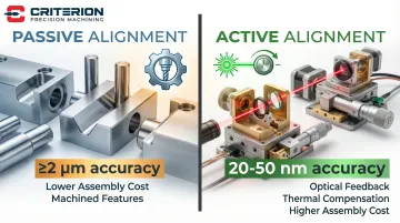
For lens centration tolerances tighter than 0.075 mm, precision machining costs for passive alignment often exceed active alignment costs — the crossover point where active alignment becomes the more economical choice.
Passive Alignment: Machining-Dependent Precision
Passive alignment places the entire alignment burden on machining accuracy and assembly precision. Typical features include:
- Precision bores sized for controlled diameter and perpendicularity to hold the lens optical axis
- Dowel pin locations machined for repeatable assembly positioning
- Reference surfaces held to tight perpendicularity and flatness to serve as optical datum planes
Advantages:
- Simpler assembly with no adjustment required
- More robust long-term stability without adjustment mechanisms
- Lower assembly cost in high-volume production
Disadvantages:
- Higher machining costs to achieve required tolerances
- Limited by practical machining precision (~2 µm floor)
- No compensation for thermal drift or assembly variations
Active Alignment: Designing for Adjustability
Active alignment incorporates adjustment mechanisms that permit post-assembly tuning while monitoring optical performance. Common mechanisms include:
- Set screws for angular tuning of mirrors and beam steering elements
- Translation stages for lateral alignment of fibers to chips
- Threaded adjusters for axial positioning of lens elements
Each mechanism imposes its own machining demands:
- Precision threads cut for smooth, backlash-free adjustment
- Flat contact surfaces ground for stable set screw engagement
- Clearances sized to allow full adjustment range without interference
High-power laser systems and research instruments — where thermal drift compensation or frequent reconfiguration is unavoidable — rely on active alignment to maintain performance over time.
Multi-Axis Alignment Complexity
Optical systems require simultaneous alignment in six degrees of freedom: X, Y, Z translation plus tip, tilt, and rotation. Machining must accommodate all adjustment mechanisms while maintaining enough structural rigidity to prevent deflection under the forces those adjustments generate.
Kinematic mounting principles address this by constraining exactly six degrees of freedom through point contacts. The Maxwell clamp (three V-grooves) and Kelvin clamp (tetrahedron-vee-flat) both deliver sub-micron repeatability even after disassembly — but only when contact surfaces and locating features are machined to correspondingly tight tolerances. For photonics assemblies, that means the machining strategy is inseparable from the alignment strategy.
Quality Assurance and Metrology
In-Process Inspection Strategies
Checking critical dimensions during machining rather than only at completion prevents scrap and reduces cost. Typical in-process checks include:
- Comprehensive dimensional verification of the first production part before the run continues
- Periodic sampling during production to detect tool wear before tolerances drift
- Profilometer checks on critical optical mounting surfaces to confirm finish requirements
Criterion builds multiple inspection checkpoints into their manufacturing sequences, catching dimensional issues before they become scrap. Their Global Advantage CMM running PC-DMIS software supports in-process measurement across production runs, giving real-time visibility into process stability.
Final Inspection and Documentation
Comprehensive final inspection for photonics components includes:
- Full GD&T dimensional report from CMM measurements with traceable calibration records
- Ra surface finish verification on all optical mounting surfaces
- Mill test reports confirming alloy composition and material certification
- Geometric tolerance verification covering perpendicularity, concentricity, flatness, and parallelism
Criterion's ISO 9001 and ISO 13485 certifications ensure documented processes at every production stage — the traceability that aerospace, defense, and medical device customers require.
Environmental Control in Inspection
Those CMM measurements are only as reliable as the environment in which they're taken. Temperature variations affect measurement accuracy at the micron level, which makes environmental control non-negotiable for photonics work. Best practices include:
- Temperature-controlled inspection rooms held at 20°C ±0.1°C with gradients no greater than 0.03°C/hour
- Adequate thermal stabilization time for both parts and measuring equipment before measurement begins
- Regular calibration of measurement equipment against traceable standards per ISO 10360
Without environmental control, thermal expansion during measurement can consume the entire tolerance budget. A 1°C temperature difference between a part and CMM creates measurement errors of 2-3 µm on a 100 mm dimension.
Frequently Asked Questions
How are precision optics made?
Precision optics manufacturing covers two areas: fabricating optical elements (grinding, polishing, coating) and machining the mechanical components that hold them. This article focuses on the mechanical side—the housings, barrels, and mounts that position lenses and mirrors with sub-micron accuracy.
What materials are used in photonics?
Common materials for photonics mechanical components include aluminum alloys (6061, 7075) for general-purpose housings due to excellent machinability and light weight, titanium for aerospace applications requiring low thermal expansion, stainless steel (303, 316) for high-stability and corrosive environments, and engineering polymers like PEEK for electrical insulation and specialized requirements. Material selection depends on thermal stability (CTE), weight constraints, machining precision requirements, and application environment.
What are the 4 types of alignment?
The four fundamental alignment types in photonics each carry different machining precision requirements and cost trade-offs:
- Passive — machined features alone determine optical alignment, no adjustment
- Active — adjustment mechanisms with optical feedback for post-assembly tuning
- Hybrid — passive features for coarse alignment, active adjustment for fine tuning
- Self-alignment — V-grooves or tapered interfaces guide components into position
What is the 3 point alignment method?
Kinematic mounting uses three precisely machined contact points to constrain a component in six degrees of freedom without over-constraint — eliminating stress from thermal expansion or manufacturing variation. Contact surfaces and locations must be machined to within 2-5 µm to achieve sub-micron repeatability after repeated disassembly and reassembly.
Photonics component machining operates on different rules than conventional precision manufacturing. When visible light operates in the 400-700 nm range, mechanical infrastructure must hold tolerances measured in microns or nanometers. Success requires understanding the relationship between mechanical precision and optical performance, selecting materials that maintain dimensional stability across temperature ranges, and implementing alignment strategies that balance machining cost with system performance.
For manufacturers serving aerospace, defense, medical device, and telecommunications sectors, partnering with a precision machining specialist experienced in photonics applications ensures that mechanical components won't compromise optical system performance. Criterion Precision Machining combines a manufacturing heritage dating to 1953 with specialized expertise in photonics, maintaining the ±0.0002" tolerances, temperature-controlled environments, and comprehensive quality systems that photonics applications demand.